

Website: www.canmtech.com
E-mail:sales@canmtech.com
Tel: 86-13682606904
Skype: lindyzhoupcb
Wechat: lindyzhousmart
Address:Room 8302, Office R&D Building, Tongzhou Electronics Longgang Factory Area, No.1 Baolong 5th Road, Baolong Community, Baolong Street, Longgang District, Shenzhen, China
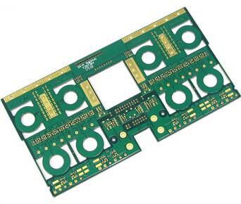
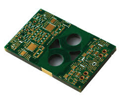
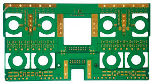
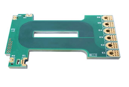
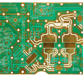
The normal copper thickness of the PCB is18μm, 35μm, but some project also need the copper foil thickness with 55um, 70um, 90um, 135um or more higher, the maximum copper thickness we can do is 6OZ(210um).
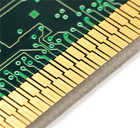
Our Inspection items for heavy copper
· 1. Check via metallization quality status to ensure there are no remains, burrs, black vias etc.
· 2. Check if substrate surface contains dirt and other remains.
· 3. Check P/N, figure number, document and process description of substrate.
· 4. Figure out the loading area and requirements of coating.
· 5. Plating area and process parameters should be clear to ensure the stability and viability of copper plating process.
· 6. Clean and preparation of conductive parts, solution activated through conductivity.
· 7. Check if solution composition is qualified and plate surface area.
· 8. Check the contact parts of the firm, the voltage and current range.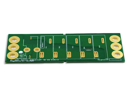
We would like to be your top choice of heavy copper PCB manufacturer,if there is any related RFQ, please contact with us at mail of: sales@canmtech.com, thank you!


 Wechat
 Online Service
 sales@canmtech.com